Biomedical Engineering Reference
In-Depth Information
Secondary flat
(001)
1 Wafer
(011)
GaAs boule
(010)
Primary flat
(011)
(100)
Z
, <001>
X
, <100>
-
Z
, <011>
Y
, <011>
-
Y
, <010>
<011>,
Y
΄
Z
, <011>
End view of guide
X
, <100>
-
^
E
= -
E
X
X
, Applied field
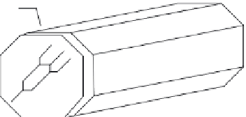
FIGURE 2.64
Crystal orientation of waveguides for the determination of electro-optic coefficients.
Substituting Equation 2.16 into Equation 2.15 yields
Δ∅ =
π
λ
r n V
l
t
3
(2.17)
41 0
As an example, we calculate the value of applied voltage necessary to induce
a phase change of π radians for a length of waveguide
l
. The material param-
eters for a GaAs waveguide are
n
0
= 3.46,
r
41
= 1.2 × 10
−12
m/V. Assuming an
operating wavelength of 850 nm and a guide thickness of
t
= 1 μm, we find
that
V
= 0.018/
l
V or, given a 1 cm electrode interaction length,
V
= 1.8 V.
2.14 NonlinearRefractiveIndex
The nonlinear refractive index is a third-order optical effect as opposed to
the Pockels effect, which is a second-order effect. The discussion that fol-
lows is intended to explain the fundamental theoretical basis of all nonlin-
earities. A wide variety of third-order nonlinear optical effects is found to be
related through the complete formalism of nonlinear optical susceptibilities.
Among these are ellipse rotation, the “dc” Kerr effect, the optical (or “ac”)
Kerr effect, self-focusing, self-phase modulation, phase conjugation, and
four-wave mixing.


Search WWH ::

Custom Search