Biomedical Engineering Reference
In-Depth Information
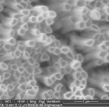
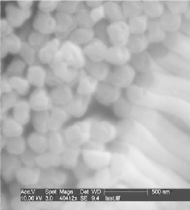
(A)
(B)
FIGURE 13.17
SEM top view of the PPy(DBS) nanowires: (A) the hollow top portion of the nanowires can
be clearly seen and (B) the nanowires have been mechanically lapped.
Porous alumina membrane
Conducting seed layer is deposited on alumina
Polypyrrole nanowires are electropolymerized in alumina pores
Sample 1: Top 15
µ
m layer
removed by mechanical
lapping
Sample 3: Au/PPy film
completely attached to a
substrate and sputtered
with second layer of Au
Sample 2: Au/PPy film
attached to a substrate
at one end
FIGURE 13.18
Schematic representation of the process fl ow seen in cross-section.
13.4.2.2 SEM Evidence of Electrochemically Induced Volume
Change in Polypyrrole Nanowires
The ability of the PPy nanowires to act as actuators was initially examined by SEM imaging. The
nanowires were left embedded in the alumina membrane and then subjected to mechanical lapping
to remove the top 10-15 µm (Figure 13.18, sample 1). The top surface was imaged with a SEM
(Figure 13.19A). As seen from the fi gure, the surface is smooth since the upper surfaces of the
nanowires are even with the top surface of the alumina membrane. This assembly (lapped alumina
membrane with embedded PPy nanowires) was placed in the NaDBS electrolyte with a platinum