Biomedical Engineering Reference
In-Depth Information
13.2.4.1
Fabrication of an Optically Controlled Polypyrrole Microstructure
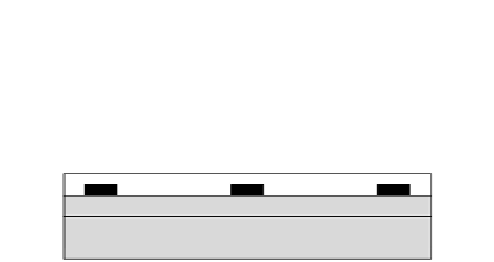
An n-type Si wafer with an implanted p-type top layer was used as a substrate. A thin metal fi lm was
deposited and patterned on the back and front sides of the substrate. A thin layer of SiO
2
was then
sputtered and patterned on the front side of the wafer to protect exposed Si surface from contact with
the electrolyte solution (Figure 13.11). A second layer of metal was deposited and patterned into 50 µm
wide strips on top of the oxide layer to provide a seed layer for PPy deposition. The two metal layers
and oxide layer were patterned such that both metal fi lms were electrically connected, thus provid-
ing PPy with an electrical contact to the p-doped side of the photodiode. PPy was electrochemically
deposited on the seed layer from an aqueous solution of pyrrole monomer to a thickness of 4 µm.
13.2.4.2
Operation of the Device
The fi nished device was placed in an aqueous solution of NaDBS and biased at
V
bias
2.25 V.
The displacement of the PPy in the direction normal to substrate surface was then measured by a
profi lometer as incident light was fi rst switched on and then switched off (Figure 13.12).
The maximum contraction or expansion of the actuator due to light modulation (
T
max
)
was measured to be
=
∼
90 nm, which is
∼
2% of the PPy thickness as deposited. As seen from
+
V
bias
−
Gold film
Polypyrrole
SiO
2
film
Si pn junction
Incident light
Electrolyte
solution
FIGURE 13.11
Operation of PPy microactuator integrated with Si photodiode.