Hardware Reference
In-Depth Information
Read cycle with 1 wait state
T
1
T
2
T
3
Φ
T
AD
ADDRESS
Memory address to be read
T
DS
DATA
Data
T
M
T
MH
MREQ
T
ML
T
RH
RD
T
RL
T
DH
WAIT
Time
(a)
Symbol
Parameter
Min
Max
Unit
T
AD
T
ML
T
M
T
RL
T
DS
T
MH
T
RH
T
DH
Address output delay
Address stable prior to MREQ
MREQ delay from falling edge of
4
nsec
nsec
nsec
nsec
nsec
nsec
nsec
nsec
2
Φ
in T
1
3
3
RD delay from falling edge of
in T
1
Data setup time prior to falling edge of
Φ
MREQ delay from falling edge of
Φ
2
in T
3
RD delay from falling edge of
Φ
in T
3
Data hold time from negation of RD
Φ
3
3
0
(b)
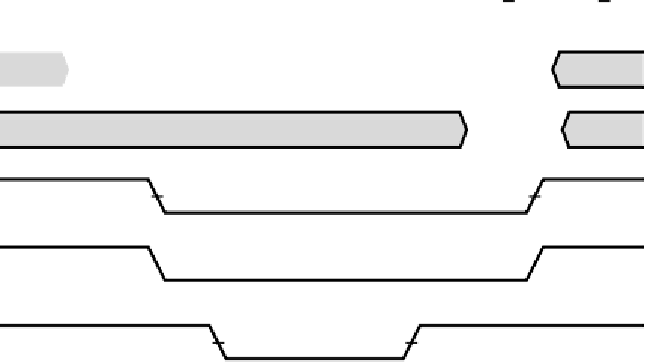
Figure 3-38.
(a) Read timing on a synchronous bus. (b) Specification of some
critical times.
down before the CPU strobes it in. The combination of constraints on
T
AD
and
T
DS
means that, in the worst case, the memory will have only 25
19 nsec
from the time the address appears until it must produce the data. Because 10 nsec
is enough, even in the worst case, a 10-nsec memory can always respond during
T
3
. A 20-nsec memory, however, would just miss and have to insert a second wait
state and respond during
T
4
.
−
4
−
2
=