Hardware Reference
In-Depth Information
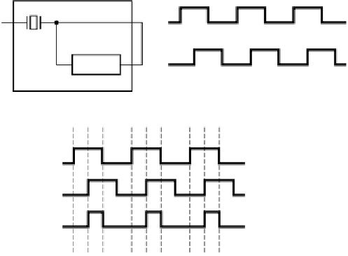
C1
C2
Delay
(a)
(b)
A
B
C
(c)
Figure 3-20.
(a) A clock. (b) The timing diagram for the clock. (c) Generation
of an asymmetric clock.
An essential component of every computer is its memory. Without memory
there could be no computers as we now know them. Memory is used for storing
both instructions to be executed and data. In the following sections we will exam-
ine the basic components of a memory system starting at the gate level to see how
they work and how they are combined to produce large memories.
To create a 1-bit memory, we need a circuit that somehow ''remembers'' previ-
ous input values. Such a circuit can be constructed from two
NOR
gates, as illus-
trated in Fig. 3-21(a). Analogous circuits can be built from
NAND
gates. We will
not mention these further, however, because they are conceptually identical to the
NOR
versions.
The circuit of Fig. 3-21(a) is called an
SR latch
. It has two inputs,
S
, for Set-
ting the latch, and
R
, for Resetting (i.e., clearing) it. It also has two outputs,
Q
and
Q
, which are complementary, as we will see shortly. Unlike a combinational cir-
cuit, the outputs of the latch are not uniquely determined by the current inputs.
To see how this comes about, let us assume that both
S
and
R
are 0, which they
are most of the time. For argument's sake, let us further assume that
Q
0. Be-
cause
Q
is fed back into the upper
NOR
gate, both of its inputs are 0, so its output,
=