Biomedical Engineering Reference
In-Depth Information
VLSI standards
1.8, 3, 5, 10 and 20
m (silicon, 2-D)
100, 200, 400, 800 and 1000 nm (silicon, 1-D)
Ted Pella
144 nm (aluminium on Silicon)
300 nm (titanium on silicon)
MikroMasch
3 and 10
m, HOPG
SPI Supplies
300 or 700 nm (metal-coated silicon)
Electron Microscopy Sciences
300 or 700 nm (metal-coated silicon)
Applied NanoStructures
3, 10, 20 and 50
m (metal-coated silicon)
Veeco
1, 2, 10, 15
m (silicon)
NT-MDT
278 nm (aluminium on glass, 1-D)
3
m (silicon, 2-D)
Asylum Research
10 and 20
m pitch (metal on silicon)
Nanosensors
100, 200 or 300 nm (silicon)
4, 8 and 16
m (silicon)
2378 nm
1-1
1-2
2-1 2-2
1783 nm
1189 nm
594 nm
0 nm
0.00 µm
3.39 µm
6.77 µm
10.16 µm
0 µm
10.16 µm
Pair 1
Pair 2
Y (µm)
Z (µm)
Y (µm)
Z (µm)
1
3.597
290.085
1487.031
2.039
2
1621.920
4.301
462.501
2.966
distance
1331.835
0.705
-1024.531
0.927
angle
55.16°
-55.49°
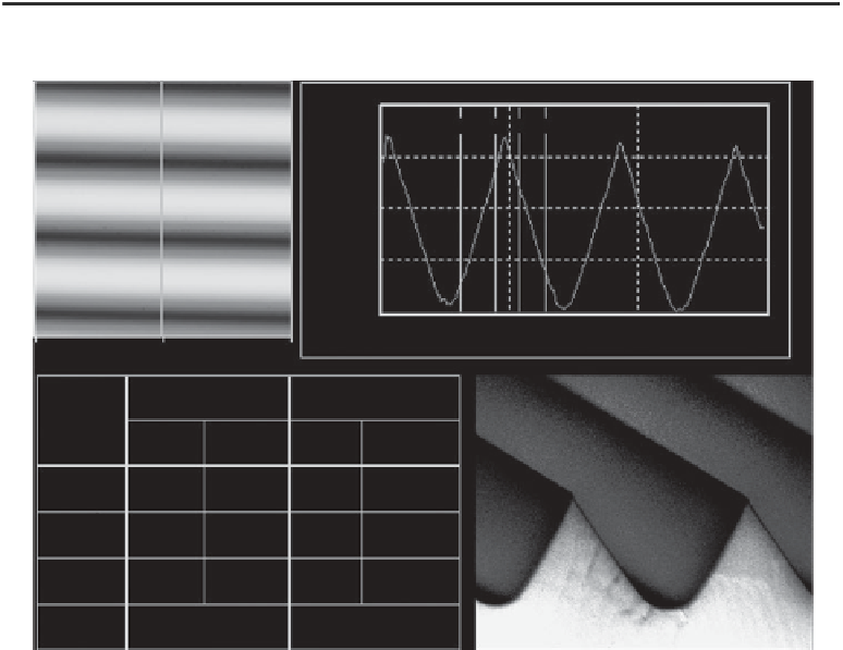
Fig. A4. Example of
XZ
or
YZ
orthogonality measurement on a triangle sample. In this case, the
AFM image (top left) shows remarkably little crosstalk between the X-Y and
Z
axes, as the measured
angles are 55.2 and 55.5
8
on the two sides of the triangle feature. At bottom right is an SEM image of
the triangle sample (TGG sample, image courtesy of Mikromasch).