Information Technology Reference
In-Depth Information
Chip manufacturers are competing to develop a nonvolatile memory chip that requires
minimal power, offers extremely fast write speed, and can store data accurately even after
a large number of write-erase cycles. Such a chip could eliminate the need for RAM and sim-
approaches to provide such a memory device.
Although microprocessor speed has doubled every 24 months over the past decade,
memory performance has not kept pace. In effect, memory has become the principal bot-
tleneck to system performance. The use of
cache memory
, a type of high-speed memory that
a processor can access more rapidly than main memory (see Figure 3.4), helps to ease this
bottleneck. Frequently used data is stored in easily accessible cache memory instead of slower
memory such as RAM. Because cache memory holds less data, the CPU can access the desired
data and instructions more quickly than selecting from the larger set in main memory. Thus,
the CPU can execute instructions faster, improving the overall performance of the computer
system. Cache memory is available in three forms. The Level 1 (L1) cache is on the CPU
chip. The Level 2 (L2) cache memory can be accessed by the CPU over a high-speed dedicated
interface. The latest processors go a step further and place the L2 cache directly on the CPU
chip itself and provide high-speed support for a tertiary Level 3 (L3) external cache.
cache memory
A type of high-speed memory that a
processor can access more rapidly
than main memory.
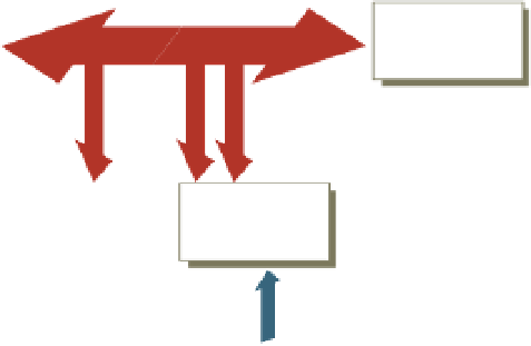
Figure 3.4
Memory
(main store)
Cache Memory
Processors can access this type of
high-speed memory faster than
main memory. Located on or near
the CPU chip, cache memory works
with main memory. A cache
controller determines how often the
data is used, transfers frequently
used data to cache memory, and
then deletes the data when it goes
out of use.
CPU
Typically
4 MB
Cache
controller
Cache
memory
Typically
256 KB
or more
Hit
Miss
When the processor needs to execute an instruction, the instruction's operation code
indicates whether the data will be in a register or in memory. If the operation code specifies
a register as the source, it is taken from there. Otherwise, the processor looks for the data in
the L1 cache, then the L2 cache, and then the L3 cache. If the data is not in any cache, the
CPU requests the data from main memory. If the data is not even stored in main memory,
the system has to retrieve the data from secondary storage. It can take from one to three clock
cycles to fetch information from the L1 cache, while the CPU waits and does nothing. It
takes 6 to 12 cycles to get data from an L2 cache on the processor chip. It can take dozens
of cycles to fetch data from an L3 cache and hundreds of cycles to fetch data from secondary
storage. Because this hierarchical arrangement of memory helps the CPU find data faster, it
bridges a widening gap between processor speeds, which are increasing at roughly 50 percent
per year, and DRAM access rates, which are climbing at only 5 percent per year.
Memory capacity contributes to the effectiveness of a CBIS. The specific applications of
a CBIS determine the amount of memory required for a computer system. For example,
complex processing problems, such as computer-assisted product design, require more
memory than simpler tasks such as word processing. Also, because computer systems have
different types of memory, they might need other programs to control how memory is
accessed and used. In other cases, the computer system can be configured to maximize mem-
ory usage. Before purchasing additional memory, an organization should address all these
considerations.