Hardware Reference
In-Depth Information
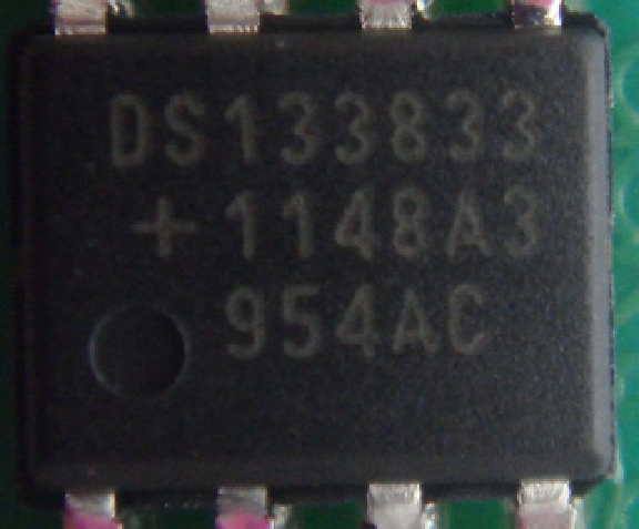
Figure 8-11.
Pin 1 indicator
This is the pad 1 indicator. You also may have noticed that the circle is about as wide as pad 1 and pad 2. Pin 1
is always the closest pad to the edge of the chip that's closest to the circle. You need to map this back to the pin leg
of your adapter board. This should be pretty easy. You can either follow the tracks on the physical board or use a
multimeter to check for continuity between the RTC chip's leg and the adapter board's leg.
It's now a good time to look at the circuit diagrams because you have all your parts assembled and ready to
use. There is one small thing you need to keep in mind: you should never place power tracks over the crystal. Nor
should you run power tracks under or close by the RTC chip. Both these components can easily be affected by outside
interference. So take a few extra moments to work out the best layout. First, let's take a look at Figure
8-12
to see how
it should be assembled on the breadboard. Unfortunately, my breadboard in real life doesn't look this neat because of
my adapter board.