Digital Signal Processing Reference
In-Depth Information
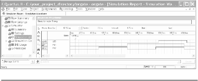
Figure 1.14
Active low OR-gate timing simulation with device time delays.
Note that the simulation includes the signal propagation timing delays through
the FPGA and that it takes almost 10 ns (ns = 10
-9
sec.) for an input change to
be reflected in the delayed output. Taking this LED output time delay into
account, examine the Simulation Waveform to verify that the LED output is
Low only when either PB1 OR PB2 inputs are Low.
1.4 Testing Your Design on an FPGA Board
The next step is to download the design to a board and test it on real hardware.
At this point, the instructions vary depending on which type of board you are
using for the tutorial. If you do not know your board type, refer back to
Figures 1.1 to 1.4 to identify it. You will need to skip ahead to the appropriate
section for each board as listed below:
•
DE1 users go to Section 1.5 (next Section),
•
DE2 users skip ahead to Section 1.6,
•
UP3 users skip ahead to Section 1.7,
•
UP2 & UP1 users skip ahead to Section 1.8.