Biomedical Engineering Reference
In-Depth Information
• Pico-satellites for space applications,
• fuel cells, and many hydraulic, pneumatic, and
• Other consumer products.
Fabrication process:
The various process steps needed to be carried out for realizing the sensor using
bulk/surface micromachining approach. The wafer serves as the substrate for
microelectronic devices built in and over the wafer and undergoes many micro
fabrication process steps such as doping or ion implantation, etching, deposition of
various materials, and photolithographic patterning.
Oxidation:
The process of oxidation consists of growing a thin film of silicon dioxide on the
surface of the silicon wafer. Oxidation is typically performed at temperatures of
900-1,200 C in the presence of O
2
(dry oxidation) or H
2
O (wet oxidation).
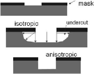
Etching Techniques:
Etching is the process of selective removal of regions of a semiconductor, metal,
or silicon dioxide. There are two types of etchings: wet and dry/Isotropic versus
Anisotropic. Figure
2.20
displays the schematic of isotropic and anisotropic thin-
film etching.
In wet etching, the wafers are immersed in a chemical solution at a predeter-
mined temperature. In this process, the material to be etched is removed equally in
all directions so that some material is etched from regions where it is to be left.
This becomes a serious problem when dealing with small dimensions.
In dry (or plasma) etching, the wafers are immersed in gaseous plasma created
by a radio-frequency electric field applied to a gas such as argon. Electrons are
initially released by field emission from an electrode. These electrodes gain kinetic
energy from the field, collide with, and transfer energy to the gas molecules, which
results in generating ions and electrons. The newly generated electrons collide
with other gas molecules and the avalanche process continues throughout the gas,
forming plasma. The wafer to be etched is placed on an electrode and is subjected
to the bombardment to fits surface by gas ions. As a result, atoms at or near the
surface to be etched are removed by the transfer of momentum from the ions to the
atoms.
Fig. 2.20 Schematic of
isotropic and anisotropic thin-
film etching
Search WWH ::

Custom Search