Biomedical Engineering Reference
In-Depth Information
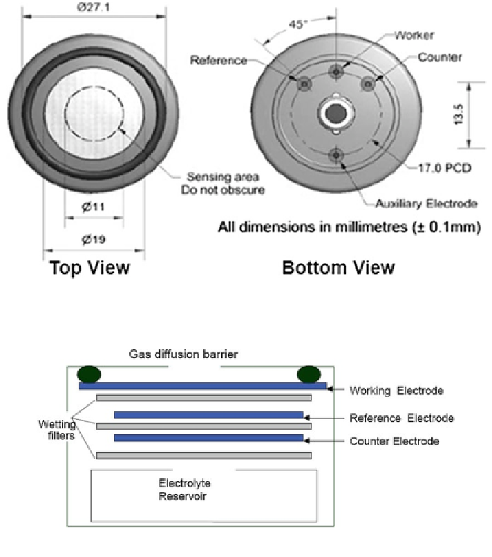
Fig. 8.4
NO-B4 schematic diagram [
46
]
Fig. 8.5
Basic structure of NOB4 [
46
]
of the circuit diagram and other details of sensor can be obtained from the man-
ufacturer's website [
47
]. Figure
8.7
shows the sensor schematic and signal con-
ditioning circuit [
47
].
TGS sensor complies with the required characteristics when the sensor is tested
in standard conditions and is specified as follows:
Test Gas Conditions: 20 ± 2 C, 65 ± 5 %R.H.
Circuit Conditions: V
C
= 15.0 ± 0.1 V (DC),
V
H
= 5.0 V DC ± 5%,
R
L
= Variable P
s
=B15mW
Conditioning period before testing: 2-7 days
Sensor Resistance (Rs) is calculated by the following formula:
Search WWH ::

Custom Search