Biomedical Engineering Reference
In-Depth Information
were subsequently performed: a second graphene sheet has been
placed at a distance of 3.35 Å below the reconstructed sheet of Fig.
5.12a, with its lateral position set to make the adsite of Fig. 5.12a
fall on an A site, and then on a B site in a separate calculation. STM
images have been recalculated from the surface electronic states of
H on bilayer graphene. The images, shown in Fig. 5.13b and c, are
practically identical to that of the single sheet case, regardless of
the adsite type, indicating that H atom adsorption, within the used
coverage and approximations, affects graphene electronics much
more strongly.
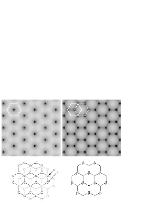
Figure
5.14
Calculated STM images for pristine carbon sheets:
(a) graphene, (b) graphite (bilayer graphene). The
hexagons at the upper left of the panels are guides for
locating carbon atoms (dashed for the subsurface C layer).
The difference between (A and B) carbon atoms are
explained through the illustrations at the bottom panel.
It should be noted that Ref. [13] suggests that single atom
adsorption images look different, depending on the atom location on
the graphite surface. Given the size and position of the STM feature
assigned the type b structure, it is plausible to interpret it as a single
adsorbed atom. However, we think that the clear lack of threefold
symmetry alone eliminates the type b feature as a singular defect,
regardless of whether it is a vacancy, atom adsorbate, or substitution.
Given the feature's size, shape, and orientation on the surface, it is
more consistent to associate the type b feature of Ref. [13] to the