Biomedical Engineering Reference
In-Depth Information
for discriminating pairs from single-point defects has been pointed
out in a previous study [28], using a superlattice.
Another point that should be emphasized here is the fact that
the two closest pairs show a marked difference in disrupting the
graphene electronics structure. The ortho pair has its hydrogen
atoms separately attached to C atoms of both substrate sublattices,
and hence the electronic states in the vicinity of the Fermi level
reveal the complete honeycomb network. However, this resulted
in a significant decrease of C atom resolution in the corresponding
simulated STM image using the chosen parameters.
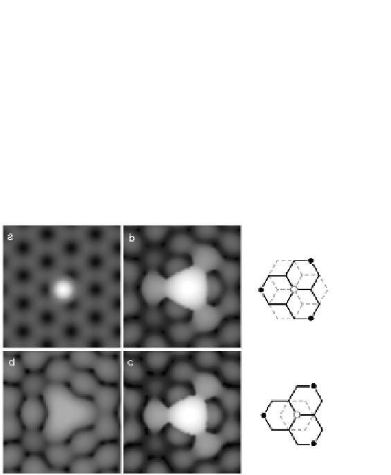
Figure 5.13
H adatom on graphene/graphite. Clockwise, from top-left:
(a) probing H adatom on single-sheet graphene using total
charge density, (b) H atom adsorbed on an A carbon atom on
two-layer graphite surface (position illustrated beside), (c)
same as (b) but on a type B carbon, (d) same as (a), but on the
reverse (clean) side of the graphene sheet. The illustrations
at the rightmost section are drawn to the same scale as the
calculated STM figures, and hydrogen is represented by the
white circle. Dashed lines indicate the positions of C atoms in
the subsurface graphene layer.
The appearance of substrate atoms from both sublattices is in
agreement with a previous STM simulation of the closest pairing p1
(dimer A) [14], but the spatial extent of the prominent STM features
differs. The adsorbed pair is represented as two distinguishable
bright spots in Ref. [14], but the image presented in this study is
more similar to a single, yet elongated, bright spot, with extensions in