Information Technology Reference
In-Depth Information
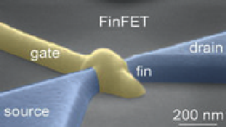
semiconductor regions. With a fin-shaped silicon channel, the flow of current
can be controlled more effectively, using all of the channel's side surfaces. Hu
explained the rationale for the fin structure as follows:
An analogy is to think of this channel like a vein. If you want to stop bleeding,
you would pinch the vein from both sides. This would be much better than
just pressing from one side.
10
Fig. 15.8. Illustration of a three-dimen-
sional FinFET transistor. Intel began
manufacturing twenty-two-nanometer
Tri-Gate transistors in 2012.
In 2000, the Berkeley researchers predicted that FinFET technology could be
scaled down to at least ten nanometers, and they estimated that such three-
dimensional transistors could move into full-scale production in about ten
years. Intel started volume production of its new twenty-two-nanometer,
three-dimensional Tri-Gate transistors in 2012 with the announcement of the
third-generation Intel Core processor family (formerly code-named Ivy Bridge).
The new three-dimensional architecture allows for a 37 percent performance
increase at low voltage and a 50 percent power reduction, compared to chips
made using conventional two-dimensional technology.
What happens after 2020 or so? Physicist Michio Kaku (
B.15.4
) has pre-
dicted the end of the “Age of Silicon”:
But this process cannot go on forever. At some point, it will be physically
impossible to etch transistors in this way that are the size of atoms. You
can even calculate roughly when Moore's law will finally collapse: when
you finally hit transistors the size of individual atoms. Around 2020 or soon
afterward, Moore's law will gradually cease to hold true and Silicon Valley
may slowly turn into a rust belt unless a replacement technology is found.
Transistors will be so small that quantum theory or atomic physics takes over
and electrons leak out of the wires. For example, the thinnest layer inside
your computer will be about five atoms across. At that point, according to
the laws of physics, the quantum theory takes over.… According to the laws
of physics, eventually the Age of Silicon will come to a close, as we enter the
Post-Silicon Era.
11
To see what might happen after 2020, we now take a quick look at three possible
postsilicon technologies.
A postsilicon age?
The ITRS roadmap is looking toward incorporating nanotechnologies onto
a CMOS silicon platform. One of the leading technologies will likely involve
new allotropes of carbon. An
allotrope
is a specific structural arrangement of
the atoms of an element in crystalline form: for carbon, the two most common
allotropes are diamond and graphite. In diamond, each carbon atom uses its
four outer electrons to bond with four other carbon atoms to form a tetrahe-
dral structure that is extremely rigid (
Fig. 15.9
). This structure gives diamond
its legendary strength and hardness. For any substance to conduct electric cur-
rent, it must contain charged particles that can move freely through the mate-
rial, such as electrons in the outer shell of an atom. In diamond, because all
four of the outer electrons in each carbon atom are tied up in bonds between
the atoms, the electrons cannot move around freely and so diamond cannot
conduct electric current. In graphite, each carbon atom uses only three of its
B.15.4. Michio Kaku is an American
theoretical physicist and popularizer
of science. He has written papers on
string theory and several popular
science topics. He has also hosted
several TV programs about science.
Kaku predicts that the end of silicon-
based computing is near.

Search WWH ::

Custom Search