Environmental Engineering Reference
In-Depth Information
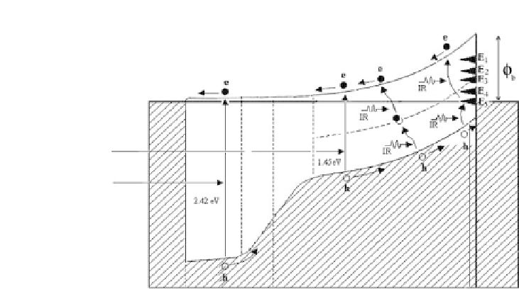
Figure 4.9
An energy band diagram of an n-CdS/n-CdTe hetero-junction
together with a large Schottky barrier at the back metal contact [8].
The final device can be completely or partially depleted, depending
on the doping concentration achieved for the CdTe layer during
growth and subsequent processing. As the energy band diagram in
Fig.4.9indicates,theinternalelectricfieldsnearthehetero-junction
and the metal/CdTe interface add up, and this becomes a tandem
solar cell. If there is good alloying at the CdS/CdTe interface during
the annealing process, the device structure is effectively a multi-
layergradedbandgaptandemsolarcellcapableofabsorbingamajor
part ofthe solar spectrum.
This new model has been formulated mainly using experimental
evidence collected by the author over a period of two decades
and valid only for high-e
ciency CdTe solar cells. The possible
band discontinuities and energy spike at the hetero-junction have
been neglected for two main reasons. The first reason is the
negligible effect of the spike at the hetero-junction when strong
band bending is present in the device structure. The second reason
is that the intermixing of materials used (CdS/CdTe) in the device
structure removes any energy spike at the boundary and produces
gradual changes in bandgaps of intermediate phases. The presence
of CdS
x
Te
(1
−
x
)
alloys in the device structure has been shown
experimentally using photoluminescence and electroluminescense