Environmental Engineering Reference
In-Depth Information
4.3.3
Effects of Defect Levels on Electronic Devices
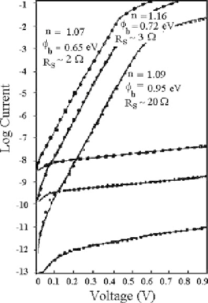
The investigation of metal/n-CdTe interfaces fabricated on chemi-
cally etched bulk CdTe surfaces revealed that the Fermi level tends
to pin at 0.72 eV on Te-rich surfaces and at
∼
0.96 eV on Cd-rich
surfaces. Detailed metal contacts on vacuum-cleaved, chemically
etched, and air-cleaved surfaces revealed that there are at least five
different Fermi-level pinning positions [7, 13, 14]. Three sets of
I-V curves showing three different pinning positions are shown in
Fig. 4.5 [7, 13, 14]. These have been observed for the same metal
gold (Au) or antimony (Sb) on the same n-CdTe bulk crystals with
only the surface preparation method beingdifferent.
Figure 4.5
Three different sets of I-V curves observed for metal/n-CdTe
bulk crystals indicating Fermi-level pinning at different positions [10].