Environmental Engineering Reference
In-Depth Information
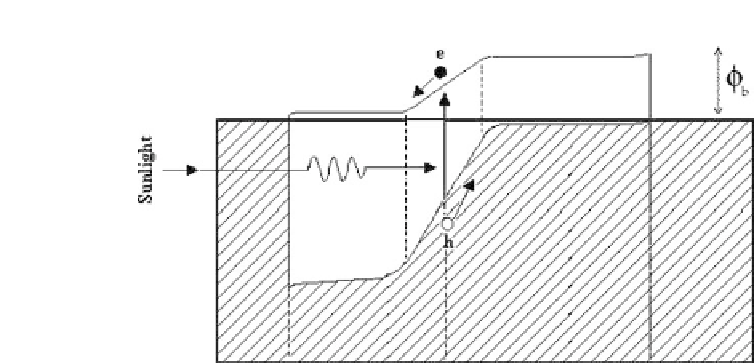
Figure 4.2
An energy band diagram of the glass/CG(metal-1)/CdS/CdTe/
metal-2 solar cell based on the p-n junction model. Note the ohmic contact
required to the p-type CdTe/metal interface according to this model (not to
scale).
post-depositionheattreatment,chemicaletching,andmetallisation.
The chemical treatment of the CdTe layer with CdCl
2
followed by
heat treatment in air at 350-450
◦
Cfor
∼
20 minutes are crucial
steps for obtaining PV activity with high e
ciencies. This device
was fabricated using electrodeposited CdTe by Basol
et al.
in the
early 1980s [5, 6], and the observed PV effect was explained in
terms of complete type conversion of the CdTe layer during the
annealing in air, forming an active p-n junction at the n-CdS/p-CdTe
interface. This original work produced an excellent device with a
goodscientificexplanationtodescribeitsaction.Researchactivities
have been carried out, and results were explained to fit with the
already accepted p-n junction model. However, the development of
thisdevicehasbeendelayedduetolackofproperexploration,inde-
pendent analysis, anddeep understanding. Comprehensive work on
metal/CdTeinterfaces[7]overthesameperiodledtotheemergence
of an alternative concept in 2002 [8] to describe the action of this
solar cell and to propose new methods of further improving its
performance.