Environmental Engineering Reference
In-Depth Information
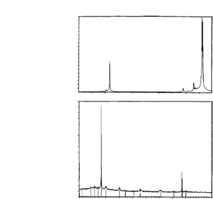
1000K
(a) MBE grown ZnSe layers on GaAs (100) surfaces
640K
360 K
160K
40K
0K
20 30 40 50 60 70
25600
(b) Electrochemically deposited ZnSe layers
on glass/ITO substrates
14400
6400
1600
0.0
20 30 40 50 60 70
[2
θ°
]
Figure 3.3
XRD patterns obtained for MBE-ZnSe layers grown on GaAs
(100) surfaces and annealed films of electrodeposited ZnSe layers grown
on glass/ITO substrates. Note that the electrodeposited ZnSe shows a high
degree of crystallinity, and only the growth orientation is different for the
two materials [15].
the composition of material layers can be produced simply by
selecting the growth voltages. Also, the possibility of formation
of different phases is evident from these experimental results.
Properoptimisationandcontrolofgrowthconditionscouldprovide
material layers with desired stoichiometry and properties. These
results indicate that the electrodeposited CuInSe
2
layers are rich in
copper at low growth voltages and rich in indium at high growth
voltages, changing the composition of the material layers.