Environmental Engineering Reference
In-Depth Information
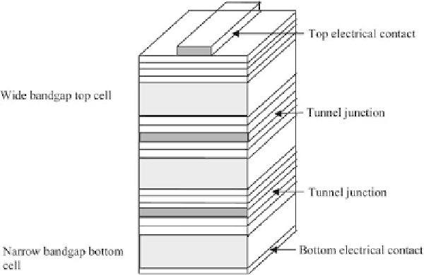
Intermediate bandgap
middle cell
Figure 2.7
Complex and expensive solar cell structures based on III-V
semiconductors, mainly developed for space applications and concentrator
solar cells.
applications. However, these devices will have applications in the
space industry and in solar panels with light concentrators. In
addition, these well-researched III-V semiconducting materials help
in the testing of new designs inPV devices.
2.5 New Technology for PV and Nano-Devices
Scientists have researched the electrodeposition of semiconductors
over the past three decades and have grown many different
semiconductors using this technique. The low cost, simplicity,
scalability, and manufacturability of this method are attractive for
large-area macroelectronic device (
∼
1m
2
) manufacturing. The
electroplating of II-VI semiconductors was first introduced by
Kroger and Pannicker [8] in the late 1970s, and BP Solar started
the scaling-up process in the mid 1980s and the manufacture of
solar panels in late 1990s. Although the device understanding was
based on a simple p-n junction during this period, solar panels
of up to 0.94 m
2
with 10.4% e
ciency were manufactured by