Environmental Engineering Reference
In-Depth Information
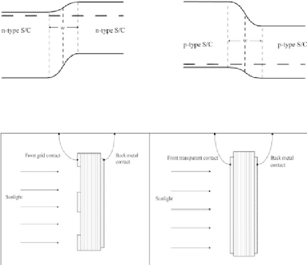
Figure 1.5
Hetero-junctioninterfacesfromn-nandp-pjunctionscreating
small steps of potentialbarriers.
Figure 1.6
Solar cells based on a grid type or transparent front contact
providing the conditions required for PV solar cells.
two electrical contacts on either side to effectively collect the
photo-generated charge carriers and transport them through an
external circuit. These electrical contacts are usually formed
using metal/semiconductor (MS), or Schottky, contacts. The front
electrical contact should either take the form of a grid contact to
minimise the effect of shading or be transparent to incoming light
(Fig. 1.6). Depending on the design of the solar cell device, the
MS interface could have either ohmic or rectifying properties. For
comprehensive information on MS interfaces, readers can refer to
textbooks written on this particular subject [13, 14].
As a brief summary of Schottky barrier formation, Fig. 1.7
presentstheenergybanddiagramofametal/n-typesemiconductor
interface. When a metal having a work function
φ
m
is brought into
intimate contact with an n-type semiconductor having an electron
a
nity
φ
b
)isformedattheinterface.If
therearenosurfacestatesorotherdefectsarisingfromthematerial,
χ
,apotentialbarrierheight(