Environmental Engineering Reference
In-Depth Information
(a)
(b)
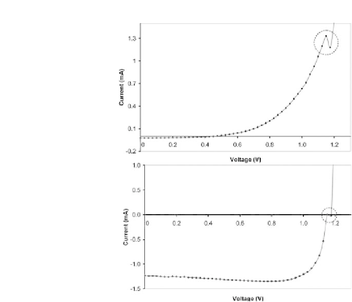
Figure 9.6
Kinks observed during I-V measurements of 0.5 mm diameter
solar cells after the application of various electrical stresses to the diode.
These kinks appear randomly at different places of the I-Vcurve.
summarisesthevariationof
V
oc
andFFvaluesobservedaftervarious
conditionsareappliedtotwo0.5mmdiametersolarcells.Figure9.9
summarises similarresults obtainedfor two 3
×
3mm
2
solar cells.
9.4.4
Discussion and Possible Explanations
It is now appropriate to discuss the defect levels present at the two
interfaces of the device under investigation. Defects on both GaAs
[10, 11] and AlGaAs [12, 13] layers have been thoroughly studied
and reported in the past, and the main electron traps are shown
in Fig. 9.10. As described before, these defect levels can drastically
affect the I-V characteristics of the device. For example, when the
Fermi level sweeps along the metal/AlGaAs interface during I-V