Environmental Engineering Reference
In-Depth Information
Fermi level moves at the interface from forward bias to reverse
bias, or vice versa. In the presence of a set of deep traps at the
interface, the Fermi level crosses these levels and allows them to
traporde-trapelectronsaccordingtothelocationofthedefectlevel
with respect to the Fermi level. This will, in turn, allow the Fermi
level to switch between defect levels and, hence, affect the
φ
b
and
the properties of I-V characteristics measured.
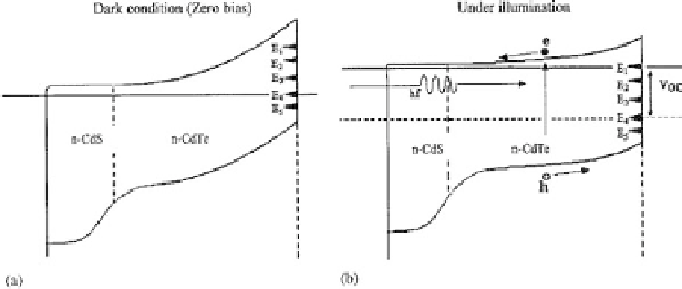
9.3 Effects on the Performance of CdS/CdTe Solar Cells
Similar variations have also been observed in fully fabricated
CdTe-based solar cells. Figure 9.3 shows the proposed energy
band diagram of the glass/TCO/CdS/CdTe/metal thin-film solar cell
according to the new model [1, 2]. For this model the CdTe layer
remains n-type with the existence of an n-n-graded hetero-junction
at the CdS/CdTe interface together with a large Schottky barrier at
the back metal contact. The defect levels E
1
-E
5
are related to native
defects,andtheirconcentrationscanbechangedbymaterialgrowth
conditions, post-growth modifications such as chemical treatments,
Figure 9.3
(a) The energy band diagram of the CdS/CdTe solar cell
accordingtothenewmodel,showingacombinationofagradedn-nhetero-
junction and a large Schottky barrier at the back metal contact. (b) Under
illumination, the device produces an open circuit voltage of
V
oc
, and this is
identical to application of a forward bias of
V
V
oc
. The pinning position
could, therefore, move upward, resulting in poor parameters for the solar
cell during the second measurement or after illumination.
=