Environmental Engineering Reference
In-Depth Information
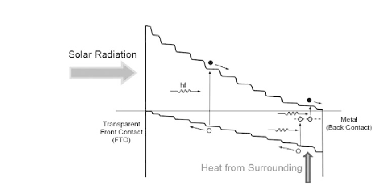
Figure 8.5
A schematic diagram showing the two energy inputs available
to this device structure. When placed in complete darkness, the device still
producesPVactivityusingtheheatenergyfromthesurroundingsduetothe
impurity PV effect.
It is interesting to note the work by Bauhuis
et al.
[7] in 2007 on
GaAs-based p-n type junctions. These devices have produced
∼
40
mAcm
−
2
for
J
sc
, and therefore GaAs is capable of producing large
short circuit current densities. As described in chapters 6, 7, and 8,
when all the desired features as shown in Fig. 8.5 are achieved to
improveopticalabsorption,incorporatingtheimpurityPVeffectand
impact ionisation to enhance
J
sc
, this parameter could attain much
largervalues.Therefore,whenfullyoptimised,thisdevicehasahuge
potentialtoincreasetheconversione
ciencyfollowingtheincrease
in
J
sc
.
8.6 Discussion
The above observations highlight the existence of two power inputs
to these graded bandgap multi-layer solar cells, as shown in Fig.
8.5, (i) the normal solar radiation when illuminated and (ii) the
surroundings of the solar cell acting as an infinite heat reservoir.
The heat from the surroundings also creates charge carriers in the