Environmental Engineering Reference
In-Depth Information
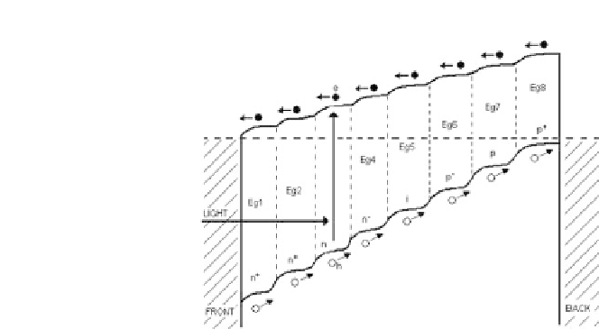
Figure 6.5
An energy band diagram of the tandem solar cell shown in
Fig. 6.4. The number of semiconductor layers included in this structure is
eight, including an n
+
-type window material.
semiconducting materials, respectively. A similar definition applies
to p-type materials, and similar structures could be built starting
from p
+
-type wide-bandgap materials. In this situation, the whole
structure can be sliced into a large number of different solar cells,
such as n
+
-n-n
−
,n
−
-i-p
−
,andp
−
-p-p
+
. The individual solar cells
are connected to form a tandem solar cell. The conduction band
of one device is connected to the conduction band of the adjacent
device;hence,theconnectionisparallel. Full absorptionofthesolar
spectrum can be achieved by gradually reducing the bandgap from
the front to the back of the solar cell, as shown in Fig. 6.5. However,
the lowest bandgap material used is a compromise since the open
circuit voltage produced by the device depends on the minimum
bandgap material used in the structure.
6.3 Comparison of the Two Connecting Methods
The two methods of connecting individual solar cells to make
tandem solar cells have their advantages and disadvantages. These
are discussed in detail in the following two sections.