Environmental Engineering Reference
In-Depth Information
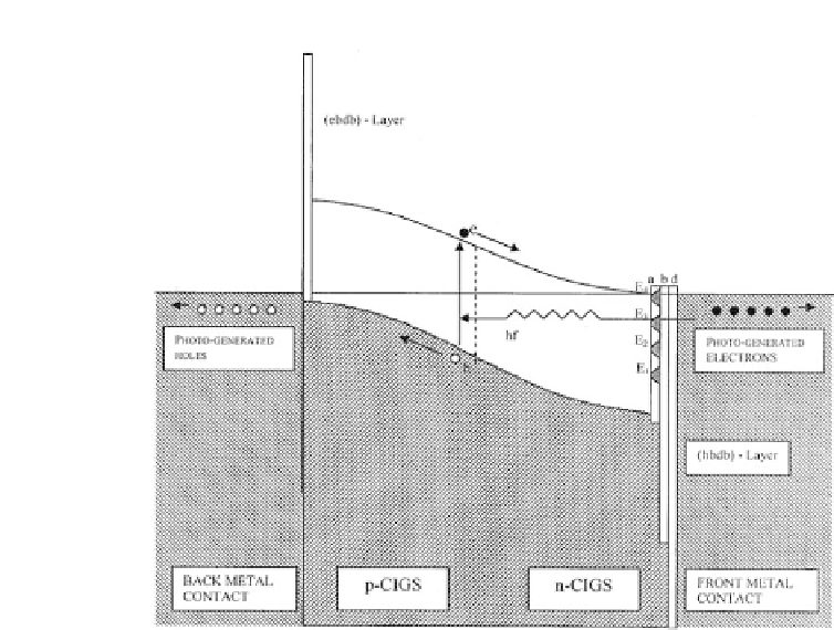
Figure 5.8
Animprovedenergybanddiagramforenhancedchargecarrier
separation and collection, incorporating ebdb and hbdb layers.
MoSe
2
attheMo/CIGSinterface.Thiscompoundisap-typematerial
withawidebandgap(
E
g
=
1
.
40eV)andsemiconductingproperties
[53-56]. These two properties, in fact, ideally produce the required
ebdb layer at the Mo/CIGS interface, as shown in Fig. 5.8. This
is another good reason for the conventional device structure to
perform well to date.
5.9 Conclusions
This chapter has summarised and presented the current knowledge
on CIGS-based material issues, device processing stages, and device
physics principles for describing CIGS-based thin-film solar cells
currently under the research and development stage. This review,
therefore, leads to the following main conclusions.