Environmental Engineering Reference
In-Depth Information
is a combination of p-n homo-junction and an MIS-type electrical
contact, improving the charge carrier creation, separation, and
collection into the external circuit.
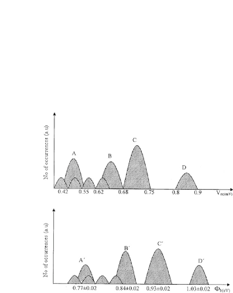
In both type-I and type-II cases, Fermi-level pinning at different
levels produces discrete
V
oc
values with varying performance. The
most desirable pinning position is at E
4
in order to produce a solar
cell with the highest
V
oc
. Since there are four possibilities for Fermi-
level pinning, four potential barriers and, hence, four groups of
V
oc
values can be expected. This has in fact been experimentally
observed, and the results are shown in Fig. 5.7. These groups can
Figure 5.7
Four different experimentally observed main groups (A, B, C,
D) of open circuit voltages and corresponding groups of potential barrier
heights possible due to Fermi-level pinning at discrete defect levels in
CIGS solar cells. Additional defect levels in the vicinity of groups A' and B',
observed by more sensitive PAS technique, are also shown.