Environmental Engineering Reference
In-Depth Information
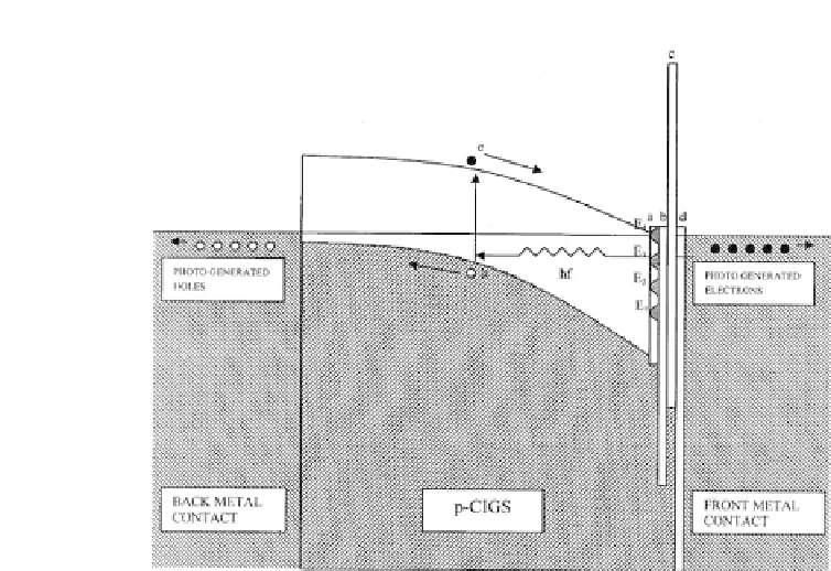
Figure 5.5
Anenergybanddiagramforthetype-Isolarcellforbackmetal
contact/p-CIGS/ODC layer(a)/n-CdS(b)/i-ZnO(c)/n-ZnO:Al(d)/front metal
contactstructure.Theconditionsshownareforshortcircuitsituationunder
illumination.
as the Fermi level. The bandgap energy values of the different mate-
riallayersareapproximatelyaccordingtoscale,andthethicknessof
CIGS(
∼
3,000nm)andthefourlayers(
∼
300nm)betweenCIGSand
the front metal contact shows a
∼
10:1 ratio in thickness. Therefore,
thedeviceisbasicallyalargeSchottkydiodeonp-CIGSwithanMIS-
type electrical contact containinga thick compound I-layer.
In theoretical modelling with ideal semiconductors, it is normal
practicetousethevacuumlevelasthereferenceenergylevelaccord-
ing to the Anderson's electron a
nity rule. Once the vacuum level
has been taken as the reference, the electron a
nity (
χ
s
) values of
semiconductors decide thelocation ofthe conductionbandminima,
resulting in band bending and, therefore, the energy band diagram.
Although this is valid for ideal situations, it is more accurate to use
theFermilevelasthereferencelevel,especiallywhentheFermilevel
is pinned in practical devices. Therefore, in this topic, all the band