Environmental Engineering Reference
In-Depth Information
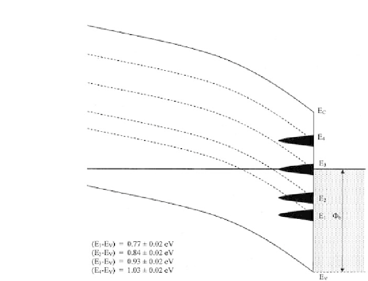
Figure 5.4
Experimentally observed Fermi-level pinning positions for
metal/p-CIGS interfaces [39].
cathodoluminescence (CL) techniques. These results are sum-
marisedinTable5.3forcomparison,anditisremarkabletoobserve
the closeness of these defect levels in CIGS material. It is also
apparent that the PAS technique is capable of identifying closely
spaced defect levels in semiconductors.
Table5.3 AsummaryofthedefectlevelsindependentlyobservedforCIGS
materials from different research groups, using six different techniques
Energy Level (eV)
Schottky Barriers [39]
PL [42]
DLTS [43]
PAS [44]
CL [45]
(I-V)
(C-V)
(E
1
-E
V
)
0.77
±
0.02
—
—
—
0.75-0.78
—
(E
2
-E
V
)
0.84
±
0.02
—
0.85
0.87
0.82-0.86
—
(E
3
-E
V
)
0.93
±
0.02
—
0.94
—
0.90
0.97
(E
4
-E
V
)
1.03
±
0.02
1.03
(1.00-1.17)
1.03
1.01
1.08