Environmental Engineering Reference
In-Depth Information
[BS-K1]
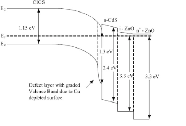
Figure 5.2
The energy band diagram used to explain the PV activity of
thin-filmCIGS solar cells.
The Fermi level should be in the middle of the energy gap for
i-ZnO,and this conditionis not satisfied here, inthis diagram.
(ii) This diagram also does not represent the actual scale of space
on the horizontal axis. In these devices, the CIGS layer is about
3,000nmandthecombined(n-CdS
+
i-ZnO
+
n-ZnO:Al)layeris
about300nminthickness.Therefore,theCIGStothecombined
layer should have the scale of 10:1 in this diagram. This real
space relationship is not shown in this diagram; therefore, it
appears to be a genuine p-n-type hetero-junction between p-
CIGSandn-CdS,providinganincorrectimpression.Whendrawn
to scale, the combined layer becomes extremely thin when
compared to the CIGS layer, indicating this as the insulating
component of an MIS-type electrical contact.
5.4 Current Views of the Physics Behind CIGS Solar Cells
It is of paramount importance to understand the solid-state physics
principles underpinning these devices in order to systematically