Environmental Engineering Reference
In-Depth Information
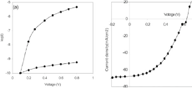
(b)
Figure 4.13
The I-V curves obtained under (a) dark and (b) illuminated
(air-mass 1.5, or AM1.5) conditions for improved devices with iodine
doping. The barrier height of 1.18 eV due to the Fermi-level pinning at the
most desired E
5
defect level and the high
J
sc
(over 60 mA/cm
2
) have been
observed. The kinks appearing on I-V curves are due to the existence of
multi-defect levels and described in details in chapter 9.
valueswereevaluatedusingthestandardmethodestablishedforthe
characterisation of Schottky contacts [36].
A typical linear-linear I-V curve under AM1.5 illumination for
these latest devices is shown in Fig. 4.13(c). The
V
oc
over 600 mV
and fill factors in the range (0.50-0.60) are typical values obtained
for these devices, but the
J
sc
(over60mA/cm
2
) is strikingly high.
Theaboveparametersproducee
cienciesof
∼
18%,whichisabove
the highest values, 16.5% reported to date [2].
The capacitance of the above structures was measured as a
function of applied bias voltage, at a measurement frequency of
1MHz.TheresultsareshowninFig.4.14,andthedevicecapacitance
remains unchanged at
∼
56 pF with the applied bias voltage. It is,
therefore, evident that the depletion width of the device structure
is greater than the combined thickness of CdS/CdTe layers. In
other words, the device structure is fully depleted, and, therefore,
the complete semiconductor layers are PV active. The calculated
geometrical capacitance of the 2 mm diameter contact is about
80 pF (assuming
ε
r
=
11forCdTeandthicknessofthedevice
=
56 pF.
Becauseaconstantcapacitanceofthesameorderasthegeometrical
2
μ
m) and comparable to the measured value of
∼