Hardware Reference
In-Depth Information
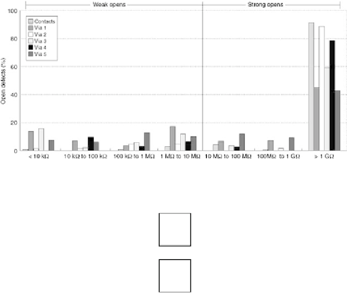
Fig. 1.9
Distribution of resistances for contact and via opens
(
Rodrıguez-Monta nes et al.
2002
)
Fig. 1.10
Interconnect
resistive
open
R
ON
R
o
n
(1-
α
)C
αC
ı
D
R
ON
C
C
R
o
.1
˛/ C
(1.6)
The factors influencing the delay added by an interconnect
resistive
open were ex-
perimentally analyzed by
Arum´ıetal.
(
2008a
)
. A set of
resistive
opens was injected
into a test chip at different locations. Furthermore, the resistance was controllable
because the opens were emulated by means of transmission gates. The delay mea-
sured on the tester for different resistances when transmitting a rising transition
metal 4 surrounded by two neighbors as close as allowed by the technology. Differ-
ent open locations were considered (RN4-RN7), where RN4 has the minimum and
RN7 the maximum coupling length, ranging from a few m until a few mm of cou-
pling length. The open resistance was controlled by the voltage of the transmission
gate terminals (x-Axis). In this way, as we move from right to left on the x-axis,
the equivalent resistance of the transmission gate increases. As expected, the delay
increases for longer coupling capacitances and also for higher open resistances.
An interconnect
resistive
open defect weakens the signal propagated through
the defective line. Thereby, the line is more vulnerable to crosstalk. Some of the