Hardware Reference
In-Depth Information
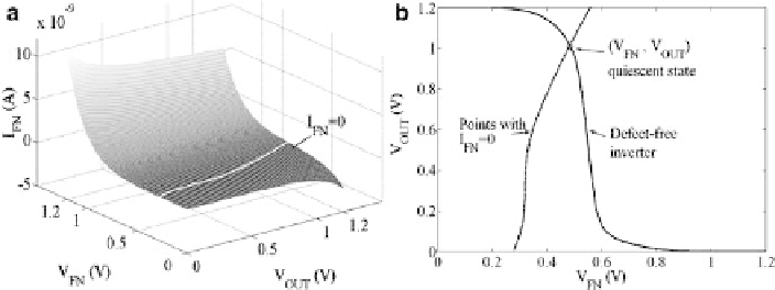
Fig. 1.6
(
a
) Sum of all the gate leakage currents .I
FN
/ at the floating input of a defective inverter,
(
b
) prediction of the steady state voltage
(
Arumı et al.
2008b
)
I
1
represents the total gate leakage currents flowing from the V
DD
rail to the floating
node. I
2
is equivalent to the total gate leakage currents flowing from the floating
node to the GND rail and I
3
stands for the total gate leakage currents flowing be-
tween the floating node and the output node of the inverter.
With the knowledge of the gate leakage currents influencing the downstream
gate, the steady state voltage of the floating line can be predicted. Assuming a float-
current .I
FN
/ at the input floating node related to the input and output voltages of
the downstream gate (inverter). The pairs (V
FN
, V
OUT
) where the resulting current
of the downstream gate is not modified, the steady state is determined by the inter-
section point between the (V
FN
, V
OUT
) pairs resulting in I
FN
D
0 and the transfer
is generated at the input (output) of the defective inverter.
1.2.1.2
Resistive Open Defects in Interconnect Lines
When open defects cause a finite increment of line resistance, they are called
resis-
tive
(or
weak
) opens. A
resistive
open weakens the affected signal, which has delay
consequences on the transient behavior of the defective circuit (
Moore et al.
2000
)
.
The electrical behavior of
resistive
opens relies on the value of the unknown
resistance. Experimental measurements were carried out by
Rodrıguez-Montanes
the open resistance values. Results showed that a high percentage of open defects
were of full nature, with resistances higher than 1 G, as illustrated in Figs.
1.8
and
opens, with resistances lower than 10 M.