Information Technology Reference
In-Depth Information
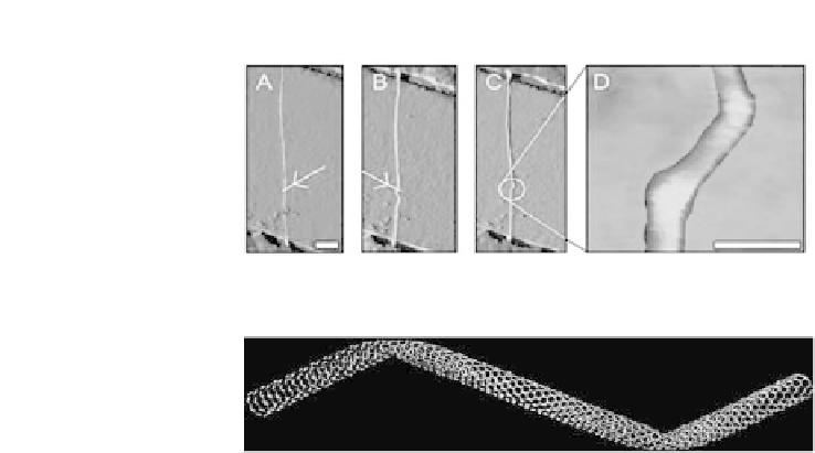
(a)
(b)
Figure
2.11.
(a) Nanotube QD fabricated by creating two kinks in the nanotube
shank using AFM manipulation. Scale bar indicates 20 nm.(From [36]. Reprinted
with permission from AAAS.) (b) Simulation of the structure Reprinted with
permission from [37] (
r
2005 American Institute of Physics)
The advantage here is that once the two nanotubes are made to cross one
another, the quantum dot is formed by the natural relaxed configuration of the
system and its size is defined automatically to be about 1.5 nm, which would be
impossible to achieve using the established patterning techniques. The effect of
this deformation on the local density of states in a similar structure was also
investigated experimentally in [39]. Thus, as can be seen, there are properties in
nanomaterials that can be capitalized on for the creation of novel devices. The
author believes that this is one of the major advantages of the world of nanoscale
devices and that many unexplored opportunities in this regard still exist.
2.4.3. Other Nanodevice Applications
2.4.3.1. Electron Emitters.
Electron emitters have long been in use in
vacuum tubes and applications such as electron microscopy and electron beam
lithography. With the advances in electron optics in these systems, the electron
emitter or source remains the performance bottleneck. Parameters such as the
brightness, energy spread, and shot noise of the electron beam directly affect
resolution, signal-to-noise ratio, and throughput in such applications. Electron
emission is the phenomenon of extracting electrons from inside a metal or
semiconductor into a vacuum. An electron emitter could be as simple as a
tungsten hairpin with a sharp point. Figure 2.13 summarizes various well
established electron emission mechanisms including emission by heating the
sample to provide the necessary kinetic energy for the electrons to overcome the


Search WWH ::

Custom Search