Information Technology Reference
In-Depth Information
separation occurs. In parallel, shear stress sensors [30] were developed to localize
arterial sites where the uptake and local oxidative degradation of trapped LDL
particles occur. The prototypes of nano- and microscale sensors will be discussed.
Both sensors provide a basis to translate model of in vitro investigation to in vivo
assessment in animal models.
Nanoscale biosensors based on individual semiconductive nanowires take the
advantage of the enormous surface-to-volume ratio of such nanostructures and
hold great promise to offer unprecedented sensitivity and response time, as well as
the capability to directly convert biological signals to electrical signals. The
feasibility of detecting LDL particles by individual In
2
O
3
(Indium Oxide) nano-
wire-based FETs in vitro has been demonstrated by Zhou and Hsiai [31, 32]. The
possibility of translating nanowire sensors to detect the oxidatively modified LDL
trapped in the atherosclerotic lesions will be a paradigm to detect, predict, and treat
individuals who are at risk for acute coronary syndromes.
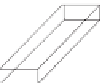
16.4.2. Nanowire and Nanotube Networked Transistors
Individual nanowire and nanotube transistors offer superior electronic character-
istics; however, device-to-device variation has been consistently observed and may
cause difficulty in the biosensing experiments. A second family of sensors—nanowire/
nanotube networked sensors—has been developed to address the above issues. These
devices have been made by controlling the density of as-synthesized nanowires/
nanotubes by tuning the catalyst density (Fig. 16.10). In
2
O
3
nanowires-based FETs
nanowire
Parylene
SiO
2
1
μ
m
(b)
Si
(a)
Ti/Au
electrodes
In
2
O
3
nanowires
Si/SiO
2
back gate
(c)
(d)
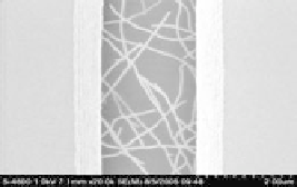
Figure
16.10.
Nanowire-based field effect transistor (FET). (a) In
2
O
3
nanowire
transistor with metal electrode passivated by parylene. (b) Scanning electron
microscope (SEM) of nanowire-based FET. (c) Concept of In
2
O
3
nanowire net-
worked transistor. (d) SEM image of the active area of one device showing
multiple In
2
O
3
nanowires bridging a pair of electrodes.


Search WWH ::

Custom Search