Information Technology Reference
In-Depth Information
14.3.2. Mapping on the Electrical VLSI Architecture
Initial Mapping. To implement our algorithm using electrical VLSI mesh, the
initial mapping to memory of each data variable is identical to the spin-
wave technique and will thus run in constant time, O(1).
Neighbor Recording. Next we store each node's right neighbor in its second
memory slot. This is still the same as in the spin-wave architecture, taking
O(1) time.
Node Elimination. Here is the main difference between spin-wave and VLSI
meshes. In the electrical VLSI, only one signal can be sent through the
channel (wire) at a time. However we can still perform the Node Elimina-
tion stage the same way as we did previously, as long as we do it for one
type of node. We can then sequentially repeat this procedure for the other
four node types. Since it took constant time for one node type, it will still
take constant time for four more node types.
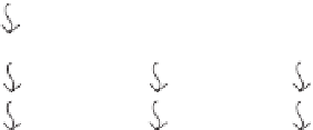
We use the third column again as our example. We turn off all switches
to force sent signals downward. We then have all the A nodes send a signal
downward and then we turn on all switches to let the signals pass. The A
nodes that do receive a signal are disabled, while the one A node that does
not receive any signals (the first and uppermost)
is chosen as the
representative node (Figure 14.7).
We repeat this process sequentially with each of the other variables (the
T, G, and C nucleotides, and the blank *). This process still runs in
constant time.
Memory Update. The last stage of updating all representative nodes' right
neighbor memory with its respective disabled nodes' right neighbors is
the same as the one shown in the spin-wave mesh. The only difference is
that since each node type does not have its own frequency, everything must
be done sequentially. However since there are only five node types, the
entire stage is still completed in constant time. Thus, the overall runtime
of the graph formation using electric VLSI will also run in constant
time, O(1).
A
A
A
*
*
*
A
A
A
A
A
A
Figure
14.7.
Disabling repeated nodes using VLSI.


Search WWH ::

Custom Search