Information Technology Reference
In-Depth Information
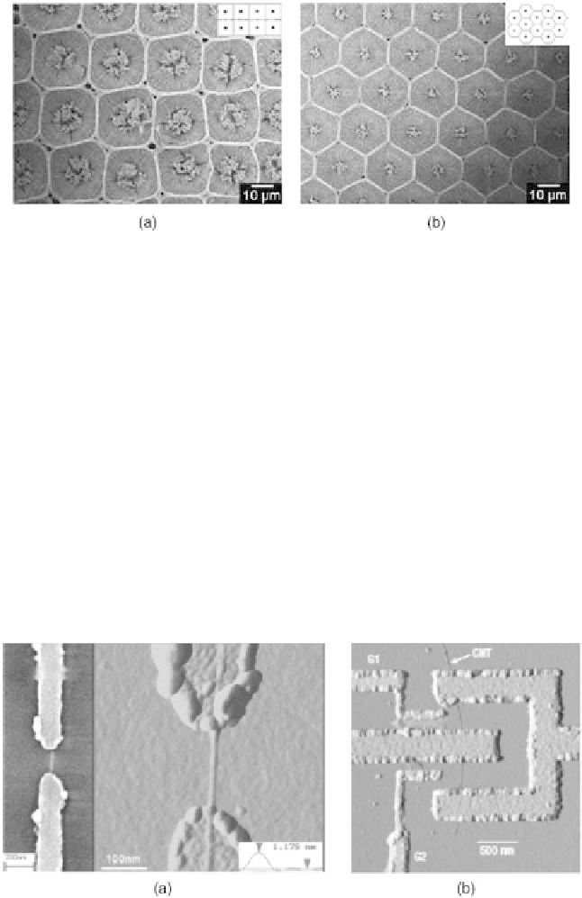
Figure
12.13.
Highly ordered carbon nanotube film patterns—(a) cubic and
(b) hexagonal—are prepared by applying capillary forces on growing carbon
nanotubes on prepatterned surfaces [35].
Within the nanometer regime, different arrangements of carbon nanotubes
have achieved on nanometer-scale electrodes of metals. Such controlled arrange-
ment foreshadows the implementation of nanotubes into device architectures that
interface the nano world with the macrosopic world. Some early examples make
use of individual carbon nanotubes as simple quantum wires by interconnecting a
pair of electrodes as depicted in Figure 12.14a [36, 37]. Based on this motif, more
elaborate device structures like transistors or SQUID loops were reported
(Fig. 12.14b,c) [38, 39]. The different kinds of CNT-based devices recently
produced represent a tool kit to interface functional molecules directly within
devices, enabling the exploitation of functionalities of molecules within the
Figure
12.14.
(a) Scanning electron microscope (SEM) (left) and STM images
(right) of an individual single wall carbon nanotube deposited onto a pair of
electrodes. Inset: an AFM profile across a carbon naotube showing its thickness
of 1.2 nm [37] (b) AFM image of a typical device geometry of the carbon
nanotube CNT-SQUID [39].


Search WWH ::

Custom Search