Information Technology Reference
In-Depth Information
Since there is no intervening oxide between the
p
-rich molecules and the silicon,
sequentially tuned molecular-structure changes can predictably regulate the device
performances over a wide range.
We have been able to prepare an electronically controlled series of molecules,
from strong
p
-electron donors to strong
p
-electron acceptors, and systematically
covalently attach them as molecular monolayers onto the channel region of pseudo-
MOSFETs (back gated). We have subsequently studied the device modulation.
We fabricated the pseudo-MOSFETs using a silicon-on insulator (SOI) wafer
(Fig. 11.9). We used this simple back-gating design instead of a more complicated
and potentially damaging top-gate fabrication in order to avoid destroying the
grafted molecules and interfering with their influence. After etching the devices in
an Ar-purged buffered oxide etch (BOE) for five minutes to remove the oxide layer
and form the H-passivated silicon surface, we grafted the molecules 1-4 (Fig.
11.10) directly onto the active area in the channel region of the device by exposing
the freshly etched samples to a 0.5mM solution of the diazonium salt (1-4)in
anhydrous acetonitrile (CH
3
CN). The grafting time depends on the molecule that
was used, and that was carefully calibrated. After grafting, we rinsed the samples
thoroughly with CH
3
CN and dried them with an N
2
flow.
We tested all the devices and measured the DC I(V) characteristics immedi-
ately after the BOE etching and before the molecular grafting. To get freshly
cleaned surface for molecular grafting, we briefly etched the devices with BOE
(30-60 s) and transferred them into the glove box for grafting. We then conducted
a second DC I(V) measurement after the grafting was completed. Devices with no
molecules (H-passivated surface) were prepared and tested as the control samples.
Both molecular grafting and testing were done at room temperature.
Grafted
Molecules
V
D
V
S
p
++
p
++
450 nm
Channel- Si
1000 nm
Si
675
μ
m
Gate-Si
200 nm
Au
500
μ
m
V
g
(a)
(b)
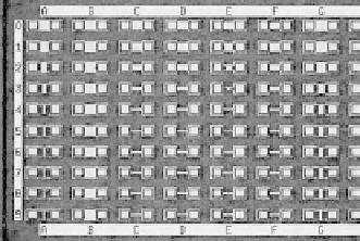
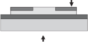
Figure
11.9.
(a) An optical micrograph of pseudo MOSFETs on one chip. Boxed
regions indicate the source and drain, between which sits the channel. The data
shown in this contribution were collected with Row 0, for which both the length
and width of the channel are 100 mm and the active area for molecular assembly
is 110110 mm
2
. (b) Schematic side-view representation (not to scale) of the
device. The molecules were grafted between source and drain electrodes. V
S
, V
D
,
and V
g
refer to the bias applied on the source, drain, and gate, respectively.


Search WWH ::

Custom Search