Information Technology Reference
In-Depth Information
ACPS line
ACPS line
ACPS line
Z
Y
10
m
10
m
50m
X
SiO
2
2
m
100 nm
Ni at Fe to ferromagnetic film
S.I. substrate
(a)
Cross-plane view
ACPS line
to excite spin wave
ACPS line
to detect the inductive voltage
ACPS line
to excite spin wave
Z
Y
SiO
2
X
Ferromagnetic film
Spin wave
S.I. substrate
(b)
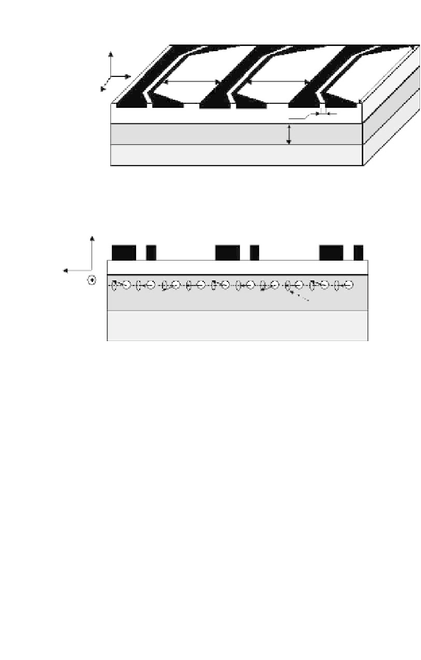
Figure
7.13.
Prototype of a spin-wave logic device.
structure. The lines and the ferromagnetic layer are isolated by the silicon oxide
layer.
The thickness of the ferromagnetic layer can be as thin as tens of nanometers,
and the thickness of the oxide layer is several hundreds of nanometers. The
dimensions of the ACPS lines are defined by the frequency of the transmitting
signal. Each of the ACPS lines can be used for spin-wave excitation and detection.
A voltage pulse applied to the ACPS line produces magnetic field perpendicular to
the polarization of the ferromagnetic film, and, thus, generates a spin wave (spin-
wave packet). Being excited, the spin wave propagates through the ferromagnetic
film. As it reaches the nearest ACPS line, the amplitude and the phase of the spin
wave is detected by the inductive voltage measurements. For example, the edge
ACPS lines can be considered as the input ports, and the ACPS in the middle as
the output port. The middle ACPS line detects the inductive voltage produced
by the superposition of two waves. Depending on the relative phase of the spin
waves, the amplitude of the inductive voltage may be enhanced (when two waves
are in phase) or decreased (when two waves are out of phase) in comparison to the


Search WWH ::

Custom Search