Information Technology Reference
In-Depth Information
Electrical characterization was performed by manually switching the electro-
des from the trapping voltage source to a measurement apparatus (Agilent
4156C). A 10-V sawtooth bias at 10Hz was used and the measured currents
were binned by voltage and averaged to remove hysteresis. Nanowire movement
in the plane of the chip during transport measurement was minimal, since
transport voltages were an order of magnitude smaller than trapping voltages.
5.3.2. Trapping Nanowire Interconnects
Nanowires up to 55
m
m in length were stably trapped, as shown in Figure 5.4b,
with noticeable bending due to the trapping field inhomogeneity. The longest
previously reported one-dimensional nanostructures to be trapped by dielectro-
phoresis at both ends were less than 15
m
m long and showed minimal bending [14].
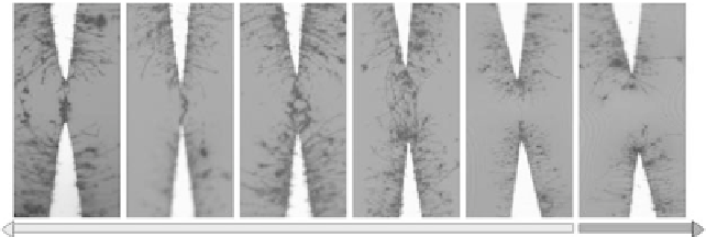
For larger electrode gaps, nanowires at either tip appeared not to experience
significant bending toward the opposite electrode, while shorter gaps caused
significant accumulations of wires, as shown in Figure 5.5.
Confirmation that the trapping voltage was not substantially attenuated was
provided by observation of a single scattering fringe around the electrodes in dark-
field mode, as shown in Figure 5.6, which was consistent with the DC Kerr effect
[6] at 155-V peak bias across a 10-
m
m gap.
The burst method was also delicate enough to enable trapping of indivi-
dual nanowires when the reservoir was diluted below 2
10
13
M, as shown in
Figure 5.7a. Before nanowire interconnects were assembled, DC transport
between electrode pairs was nearly ohmic, as shown in Figure 5.7b. The measured
current of 0.3
m
A at 1-V bias and 40-V/s sweep rate was consistent with
electrooxidation of benzyl alcohol [26, 27] at 1-
m
m-radius electrode tips.
However, after a 50-
m
m-long nanowire was trapped, the conductance became
nonlinear and showed a 50% enhancement at 10-V bias, as shown in Figure 5.7c.
Treating the device as an electrooxidative resistance in parallel with a series
nanowire resistance and Schottky contacts [28], a nanowire transport curve was
calculated, as shown in Figure 5.7d. The nanowire exhibited a calculated linear
10
μ
m
20
μ
m
30
μ
m
40
μ
m
60
μ
m
80
μ
m
Figure
5.5.
Nanowires trapped by electrodes separated by various distances.


Search WWH ::

Custom Search