Hardware Reference
In-Depth Information
t
WC
Address
t
AW
t
WR
CS
t
CW
t
AS
t
WP
WE
t
DW
t
DH
Data In
Valid data
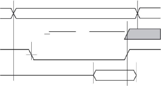
Figure 14.37c
■
K6R1008C1D write cycle timing diagram (CS controlled)
K6R1008C1D-10
Parameter
Description
Unit
Min
Max
Read Cycle
t
RC
t
AA
t
OH
t
CO
t
OE
t
OLZ
t
OHZ
t
LZ
t
HZ
t
PU
t
PD
Read cycle time
Address to data valid
Data hold from address change
CS low to data valid
OE low to data valid
OE low to low Z
OE high to high Z
CS low to low Z
CS high to high Z
CS low to power-up
CS high to power-down
10
-
3
-
-
0
-
3
-
0
-
-
10
-
10
5
-
5
-
5
-
10
ns
ns
ns
ns
ns
ns
ns
ns
ns
ns
ns
Write Cycle
t
WC
t
CW
t
AW
t
AS
t
WP
t
WP1
t
DW
t
DH
t
OW
t
WHZ
t
WR
Write cycle time
CS low to write end
Address valid to end of write
Address setup to write start
WE pulse width (OE high)
WE pulse width (OE low)
Data setup to write end
Data hold from write end
WE high to low Z
WE low to high Z
Write recovery time
10
7
7
0
7
10
5
0
3
0
0
-
-
-
-
-
-
-
-
-
5
-
ns
ns
ns
ns
ns
ns
ns
ns
ns
ns
ns
Table 14.10
■
K6R1008C1D read and write timing parameters


Search WWH ::

Custom Search