Hardware Reference
In-Depth Information
In case of more than one buffer having the same lowest priority, the message buffer with
the lowest index number wins.
T
IME
-
STAMP
R
EGISTER
(TSRH, TSRL)
If the TIME bit of the CAN
x
CTL0 register is set to 1, the MSCAN will write a special time-
stamp to the respective registers in the active transmit or receive buffer as soon as a message
has been acknowledged on the CAN bus. The timestamp is written on the bit sample point for
the recessive bit of the ACK delimiter in the CAN frame. In the case of a transmission, the CPU
can only read the timestamp after the respective transmit buffer has been flagged empty.
The timer value used for stamping is taken from a free-running internal CAN bit clock.
A timer overrun is not indicated by the MSCAN. The contents of the timestamp registers are
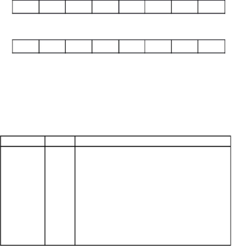
shown in Figure 13.36. The contents of timestamp registers are not sent out to the CAN bus.
7
6
5
4
3
2
1
0
TSR15
TSR14
TSR13
TSR12
TSR11
TSR10
TSR9
TSR8
TSRH
Reset:
x
x
x
x
x
x
x
x
7
6
5
4
3
2
1
0
TSR7
TSR6
TSR5
TSR4
TSR3
TSR2
TSR1
TSR0
TSRL
Reset:
x
x
x
x
x
x
x
x
Figure 13.36
■
MSCAN timestamp registers
To facilitate access to the CAN buffers, the variable names for the transmit buffer and re-
ceive buffers are added to the
hcs12.inc
file for the assembly language and the
hcs12.h
file for
the C language. These variable names are listed in Table 13.2a and b.
Name
Address
Description
CAN
x
RIDR0
CAN
x
RIDR1
CAN
x
RIDR2
CAN
x
RIDR3
CAN
x
RDSR0
CAN
x
RDSR1
CAN
x
RDSR2
CAN
x
RDSR3
CAN
x
RDSR4
CAN
x
RDSR5
CAN
x
RDSR6
CAN
x
RDSR7
CAN
x
RDLR
$_0
$_1
$_2
$_3
$_4
$_5
$_6
$_7
$_8
$_9
$_A
$_B
$_C
CAN foreground receive buffer x identifier register 0
CAN foreground receive buffer x identifier register 1
CAN foreground receive buffer x identifier register 2
CAN foreground receive buffer x identifier register 3
CAN foreground receive buffer x data segment register 0
CAN foreground receive buffer x data segment register 1
CAN foreground receive buffer x data segment register 2
CAN foreground receive buffer x data segment register 3
CAN foreground receive buffer x data segment register 4
CAN foreground receive buffer x data segment register 5
CAN foreground receive buffer x data segment register 6
CAN foreground receive buffer x data segment register 7
CAN foreground receive buffer x data length register
1. x can be 0, 1, 2, 3, or 4,
2. The absolute address of each register is equal to the sum of the base address of the
CAN foreground transmit buffer x and the address field of the corresponding register.
Table 13.2a
■
CAN foreground receive buffer x variable names
Search WWH ::

Custom Search