Hardware Reference
In-Depth Information
According to Figure 10.18, the user needs to represent the value to be converted in 12 bits
and set the most significant 4 bits properly to select the channel, shutdown mode, gain, and
reference voltage buffer mode.
Assume we want to generate a 3-V output from the
V
OUTA
pin, the value to be sent to the
MCP4922 can be calculated as follows:
•
Select channel A (set bit 15 to 0)
•
Select unbuffered mode (set bit 14 to 0)
•
Set gain to 1 (set bit 13 to 1)
•
Enable output buffer (set bit 12 to 1)
•
3 V corresponds to the digital value (lowest 12 bits) of 2
12
* 3/5 5 2458 5 0x99A
•
The value to be sent to MCP4922 is 0011 1001 1001 1010 5 0x399A
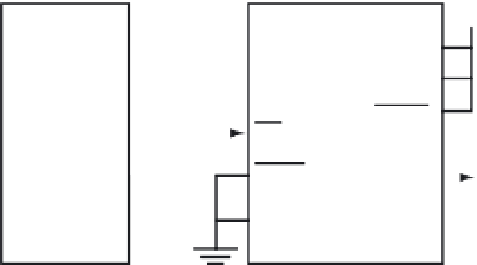
A typical circuit connection for interfacing the HCS12 wit
h t
he MCP4922 is shown in
Figure 10.19. Two unused I/O port pins must be used to drive the CS and FS pins.
HCS12
MCP4922
5 V
MOSI
SDI
V
DD
V
REFA
SCK
SCK
SHDN
PK7
CS
LDAC
V
OUTA
AVSS
Figure 10.19
■
Circuit connection between the
HCS12 and MCP4922
Example 10.7
▼
Write a program to generate the waveform from the
V
OUTA
pin shown in Figure 10.20 using
the circuit shown in Figure 10.19 assuming that the E-clock frequency for the HCS12 is 24 MHz.
4.5 V
3.0 V
1.5 V
1 ms 1 ms 1 ms 1 ms 1 ms 1 ms 1 ms 1 ms 1 ms
Figure 10.20
■
Waveform to be generated


Search WWH ::

Custom Search