Hardware Reference
In-Depth Information
If the SPI is configured as a slave, any transmission and reception in progress
continues if the SCK continues to be driven from the master. This keeps the slave
synchronized to the master and the SCK.
SPI
IN
S
TOP
M
ODE
The stop mode is dependent on the system. The SPI enters stop mode when the module
clock is disabled. If the SPI is in master mode and exchanging data when the CPU enters stop
mode, the transmission is frozen until the CPU exits stop mode. After exiting stop mode, data
to and from the external SPI device is exchanged correctly. In slave mode, the SPI will stay syn-
chronized with the master. The stop mode is equivalent to the wait mode with the SPISWAI
bit set except that the stop mode is dependent on the system and cannot be controlled with the
SPISWAI bit.
In a system that uses the SPI subsystem, one device (normally a microcontroller) is config-
ured as the
master
and the other devices are configured as
slaves
. Either a peripheral chip or a
HCS12 can be configured as a slave device. The master SPI device controls the data transfer and
can control one or more SPI slave devices simultaneously.
In a single-slave configuration, the circuit would be connected as shown in Figure 10.8. If
the SS
x
output enable feature is set, then the SS
x
pin will automatically go low to enable the
slave device before the data transfer is started. This feature is not used in Figure 10.8.
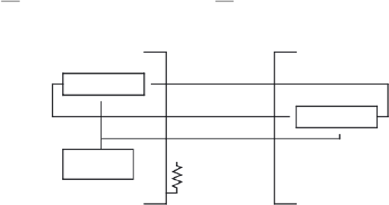
Master SPI
Slave SPI
MISO
MISO
Shift register
MOSI
MOSI
Shift register
SCK
SCK
V
DD
Baud rate
generator
SS
SS
Figure 10.8
■
Master/slave transfer block diagram
There could be several connection methods in a multislave SPI environment. One possibil-
ity is shown in Figure 10.9. In this connection method, the HCS12 can choose any peripheral
device for data transfer. In Figure 10.9, Port P pins are used to drive the SS inputs of peripheral
devices. Any other unused general-purpose I/O pins can be used for this purpose.
If we don't need the capability of selecting an individual peripheral device for data transfer,
then the connection shown in Figure 10.10 can be used, which will save quite a few I/O pins.
Figure 10.10 differs from Figure 10.9 in the following ways:
1. The MISO pin of each slave is wired to the MOSI pin of the slave device to its right.
The MOSI pins of the master and slave 0 are still wired together.


Search WWH ::

Custom Search