Hardware Reference
In-Depth Information
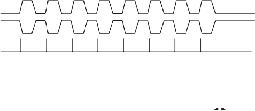
After the 16th (last) SCK edge, the SPIF flag in the SPI
x
SR register is set, indicating that the
transfer is complete. The timing diagram for this transfer format (CPHA bit 5 0) is shown in
Figure 10.5.
Begin
End
Transfer
SS (O)
master only
SS (I)
SCK (CPOL = 0)
SCK (CPOL = 1)
Sample I
MOSI/MISO
Change O
MOSI Pin
Change O
MISO Pin
t
L
t
T
t
I
t
L
Bit 6
Bit 2
Bit 5
Bit 1
Bit 6
MSB first (LSBF = 0)
LSB first (LSBF = 1)
MSB
LSB
Bit 5
Bit 2
Bit 4
Bit 3
Bit 3
Bit 4
LSB
MSB
Minimum 1/2 SCK
for
Bit 1
t
T
,
t
I
,
t
L
Figure 10.5
■
SPI clock format 0 (CPHA
5
0)
Some peripheral devices require the first SCK edge to appear before the first data bit be-
comes available at the data out pin; the second edge clocks data into the system. In this format,
the first SCK edge is issued by setting the CPHA bit at the beginning of the 8-cycle transfer
operation. The first edge of SCK occurs immediately after the half SCK clock cycle synchroni-
zation delay. This first edge commands the slave to transfer its most significant data bit to the
serial data input pin of the master. A half SCK cycle later, the second edge appears on the SCK
pin. This is the latching edge for both the master and slave. When the third edge occurs, the
value previously latched from the serial data input pin is shifted into the least significant bit
of the SPI shifter. After this edge, the next bit of the master data is shifted out of the serial data
output pin of the master to the serial input pins on the slave.
This process continues for a total of 16 edges on the SCK line with data being latched
on even-numbered edges and shifting taking place on odd-numbered edges. Again, the SPIF
flag is set after the 16th SCK edge. The timing diagram of this transmission format is shown in
Figure 10.6.


Search WWH ::

Custom Search