Hardware Reference
In-Depth Information
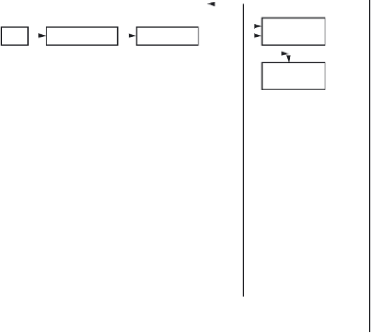
8-bit pulse accumulators can be concatenated into a single 16-bit pulse accumulator. PAC3 and PAC2
can be concatenated into the 16-bit pulse accumulator A (PACA), whereas PAC1 and PAC0 can be
concatenated into the 16-bit pulse accumulator B (PACB). The block diagrams of four 8-bit pulse
accumulators and two 16-bit pulse accumulators are shown in Figures 8.25 and 8.26, respectively.
Load holding register
and res
et pulse accumulator
0
8-bit PAC0
(PACN0)
EDG0
PT0
Edge detector
Delay counter
PA0H holding
register
Interrupt
0
8-bit PAC1
(PACN1)
EDG1
PT1
Edge detector
Delay counter
PA1H holding
register
0
8-bit PAC2
(PACN2)
EDG2
PT2
Edge detector
Delay counter
PA2H holding
register
Interrupt
0
8-bit PAC3
(PACN3)
EDG3
PT3
Edge detector
Delay counter
PA3H holding
register
Figure 8.25
■
Block diagram of four 8-bit pulse accumulators
There are four possible configurations for these pulse accumulators.
•
Two 16-bit pulse accumulators PACA and PACB
•
One 16-bit pulse accumulator PACA and two 8-bit pulse accumulators PAC1 and
PAC0
•
One 16-bit pulse accumulator PACB and two 8-bit pulse accumulators PAC3 and
PAC2
•
Four 8-bit accumulators PAC3,PAC0
Four 8-bit pulse accumulators PAC3,PAC0 are sharing the signal pins PT3,PT0 with the
lower four input-capture modules IC3,IC0, one pin per pulse accumulator. However, when concat-
enated into a 16-bit pulse accumulator, PACA and PACB use signal pins PT7 and PT0, respectively.


Search WWH ::

Custom Search