Biomedical Engineering Reference
In-Depth Information
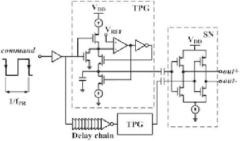
Fig. 2
Schematics of the
pulse generator (
TPG
is for
'triangular pulse generator',
SN
is for 'shaping network')
which is obtained assuming that the amplified echo has the same shape of the trans-
mitted pulse (i.e., the same of the local replica), but different amplitude (
α
is the
attenuation factor,
A
is the correlation voltage gain,
B
is the bandwidth of the low-pass
filter, and
δ
the relative delay between the input signals of the multiplier).
Building Blocks
The schematic of the building blocks (PG, LNA, multiplier, DG, and integrator)
of the SoC UWB pulse radar of Fig.
1
a are reported hereinafter, together with a
short description of the circuit design and performance. All the circuits are supplied
with 1.2 V. Receiver and transmitter have been implemented according to a fully
differential topology in order to increase the immunity to common mode noise and
interferences.
The schematic of the PG is shown in Fig.
2
. The PG has been designed by follow-
ing the principles reported by Zito et al. [
10
]. It provides a monocycle pulse on a 100
differential load (i.e., the impedance of the antenna) when activated by the negative
edge of the digital signal command occurring at
f
PR
. The measurements show a dura-
tion time (
t
D
) of the pulse of 350 ps and a pulse amplitude of 650 mV
pp
−
diff
(including
the losses of microprobes and cables) corresponding to about 900 mV
pp
−
diff
on chip.
The energy consumption (E
C
) per transmitted pulse is 19.8 mW
6.9 pJ.
The measured pulses and its PSD are shown in Fig.
3
. The power consumption is
equal to 19.8 mW. The circuit schematic of the shaper block follows the same prin-
ciple of the PG, but it requires a lower bias current (2 mA) for its shaping network
since it has a higher load impedance (i.e., the input impedance of the multiplier).
The power consumption of the shaper amounts to 13.8 mW.
The schematic of the UWB LNA is shown in Fig.
4
. The LNA has been designed
according to the design in Pepe and Zito [
11
]. It consists of a common-gate stage,
which realizes a wideband input impedance matching to the 100
differential an-
tenna load, and two subsequent common-source stages which increase the overall
gain. The measured performances of the LNA as a stand-alone circuit are shown
in Fig.
5
.S
21
is equal to 22.7 dB at 5 GHz, S
11
is lower than
×
350 ps
=
−
10.5 dB and noise
Search WWH ::

Custom Search