Biomedical Engineering Reference
In-Depth Information
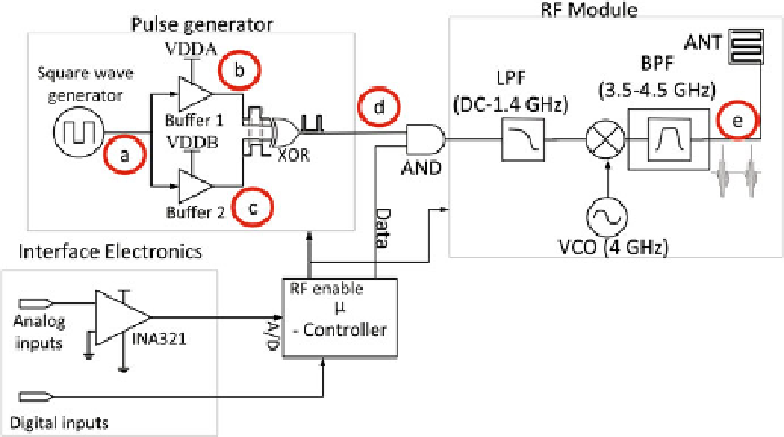
Fig. 8
VCO-based UWB sensor node design
delayed version of the input clock pulse to appear at one of the input port of the
XOR gate. Figure
7
illustrates the generation of a 1.5-ns pulse using unequal supply
voltages (
V
DDB1
=
3 V). Apart from adjustable pulse width, the
pulse repetition frequency (PRF) and pulse amplitude can also be varied to meet
the different operating requirements. The PRF is varied by changing the oscillator
output, while the adjustment of the amplitude is performed by changing
V
DDC
.
The key advantages of the pulse generator mentioned herein are the ability to vary
the pulse width, PRF, and pulse amplitude. This allows optimizing the transmitter
operation in various environments. It is important to note that the ability to change
the PRF in the suggested sensor nodes enables the system to vary the number of
UWB pulses that are used to represent a data bit [
3
,
37
].
3.3 V and
V
DDB2
=
UWB RF Module
This section analyzes two implementation methods for the UWB RF module
converting the baseband pulses into the RF domain.
VCO-Based RF Module
Figure
8
shows the implementation of the VCO-based UWB sensor node design. In
this design, the baseband USB pulses are up-converted using a VCO and a mixer.
This sensor design uses the higher power contained within the first frequency lobe
of the UWB pulse spectrum as an alternative to the amplification of the lower power
Search WWH ::

Custom Search