Biomedical Engineering Reference
In-Depth Information
a
d
g
6
3
0
0
250
500
750
Distance (nm)
b
e
h
6
3
0
0
250
500
750
Distance (nm)
c
f
i
6
3
0
150 nm
0
250
500
750
Distance (nm)
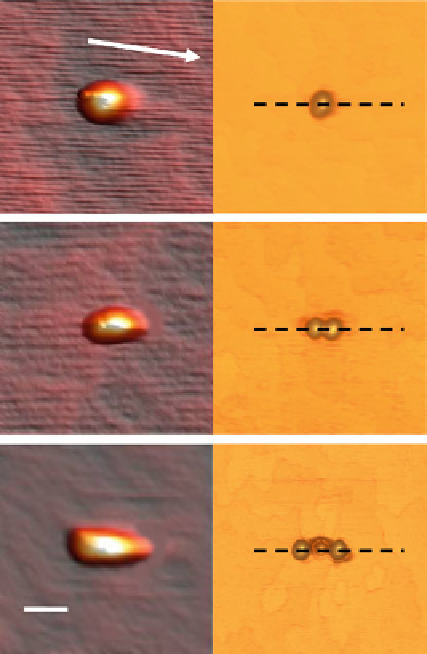
Fig. 1.16
AFM topography images of initial oxide dots with lateral dimensions 160 nm
×
160 nm
(
a
)
and
oxide
lines
fabricated
closely
along
[1 1 0]
direction
with
lateral
dimensions
160 nm
270 nm (
c
). The obtained results after deposition of 1.5 ML
of InAs on samples without GaAs buffer layer growth are shown in (
d
-
f
). The profiles along the
lateral arrangement of QDs are depicted in (
g
-
i
). Adapted from [
22
]. Copyright 2009 Institute of
Physics
×
230 nm (
b
) and 160 nm
×
the B-slope areas inside the stripes, the incorporation rate of In atoms inside this
pattern increases, which finally determines the selectivity of the pattern for the
InAs nucleation process. Taking into account these findings, it can be inferred
that the amount of InAs (i.e., number of QDs formed inside the nanohole) can
be controlled by previously designing the nanohole size and shape during the
lithography process. Figure
1.16
shows AFM images of the initial oxide dots with
lateral dimensions 160 nm
160 nm (Fig.
1.16
a), and oxide lines fabricated closely
along the [1 1 0] direction with lateral dimensions 160 nm
×
×
230 nm (Fig.
1.16
b),
and 160 nm
270 nm (Fig.
1.16
c). The height of both, the oxide dots and the lines,
is about 8 nm. The results obtained after deposition of 1.5 ML of InAs on these
×