Biomedical Engineering Reference
In-Depth Information
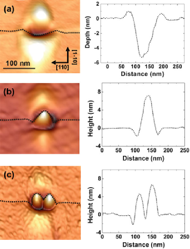
Fig. 1.7
3D rendered AFM images of a typical (
a
) nanohole, (
b
) single QD, and (
c
) QDM obtained
by droplet epitaxy etching technique and posterior preferential nucleation of InAs material. Profiles
on these nanostructures along the GaAs [1 1 0] direction are shown at the
right
. Reprinted (adapted)
with permission from [
20
]. Copyright 2009 American Chemical Society
III atoms (Ga and In) into the nanoholes for the different As
2
pressures used in each
case. In this regard, special relevancy has the crystalline orientation of the facets
defined inside the nanoholes, which eventually conditions the nucleation process
of In atoms [
22
]. On patterned substrates, apart from the GaAs (0 0 1) surface,
two different surfaces can be identified: (0 0 1) disoriented surfaces towards [1 1 0]
direction with step edges parallel to this direction that are Ga-terminated (A-type
facets), and (0 0 1) disoriented surfaces towards [1
−
1 0] direction with step edges