Biomedical Engineering Reference
In-Depth Information
-50 mV, showing a sharp ~52 mV drop within 250 ms after
cell/tip contact. During recording, the potential maintained at a
relatively constant value of ca. -46 mV, and returned to baseline
when the cell was detached. Interestingly, nanoFET probes of sim-
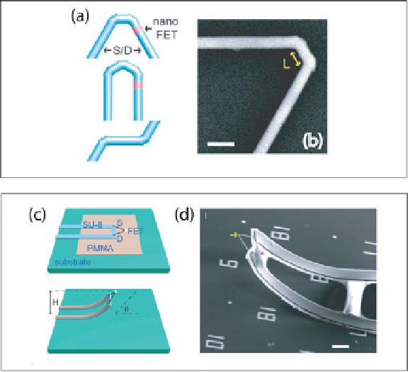
Figure 8. 3D kinked nanowire probes. (a) Schematics of 60° (top) and 0° (middle)
multiply kinked nanowires and cis (top) and trans (bottom) configurations in nan-
owire structures. The blue and pink regions designate the source/drain (S/D) and
nanoscale FET channel, respectively. (b) SEM image of a doubly kinked nanowire
with a cis configuration. (c) Schematics of device fabrication. Patterned poly
(methylmethacrylate) and SU-8 microribbons serve as a sacrificial layer and flexi-
ble device support, respectively. The dimensions of the lightly doped n-type silicon
segment (white dots) are ~80 by 80 by 200 nm
3
. H and q are the tip height and
orientation, respectively, and S and D designate the built-in source and drain con-
nections to the nanoscale FET. (d) SEM image of an as-made device. The yellow
arrow and pink star mark the nanoscale FET and SU-8, respectively.
Search WWH ::

Custom Search